The exponential growth of AI and high-performance computing is pushing data centers to their limits. With bandwidth demands soaring to 800G, 1.6T and even 3.2T, traditional optic transceivers face significant challenges in power consumption, density,cost. Enter Silicon Photonics—a disruptive technology that integrate optical components directly onto silicon substrates. In the blog, HYTOPTODEVICE, A Professional Optical Transceiver Provider, will explore challenge and develop of Silicon Photonics
Table of Contents
一、What is Silicon Photonics?
二、Silicon Photonics Transceivers: Architecture & Advantages
三、Key Benefits of Silicon Photonics Transceivers
四、Challenges in Silicon Photonics
五、Applications of Silicon Photonics
六、Conclusion
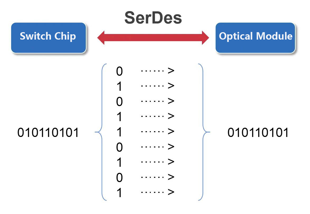
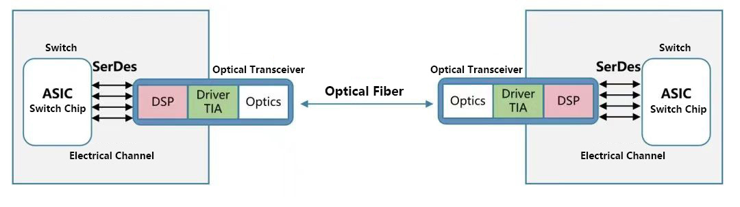
一、What is Silicon Photonics? In traditional optical communication systems, fiber optical transceivers act as "electro-optical converters," switching between electrical and optical signals. These signals travel via fiber optics between devices, while Serializer/Deserializer (SerDes) circuits handle electrical signaling within equipment. However, SerDes has become a bottleneck at multi-gigabit speeds due to signal degradation over longer distances.
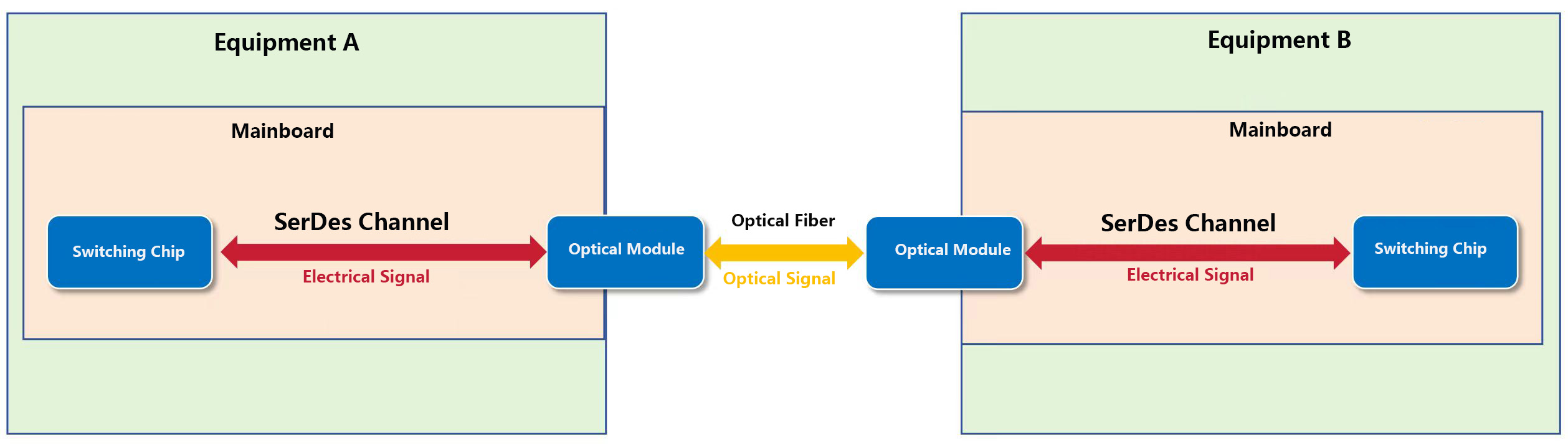
Silicon Photonics tackles this by:
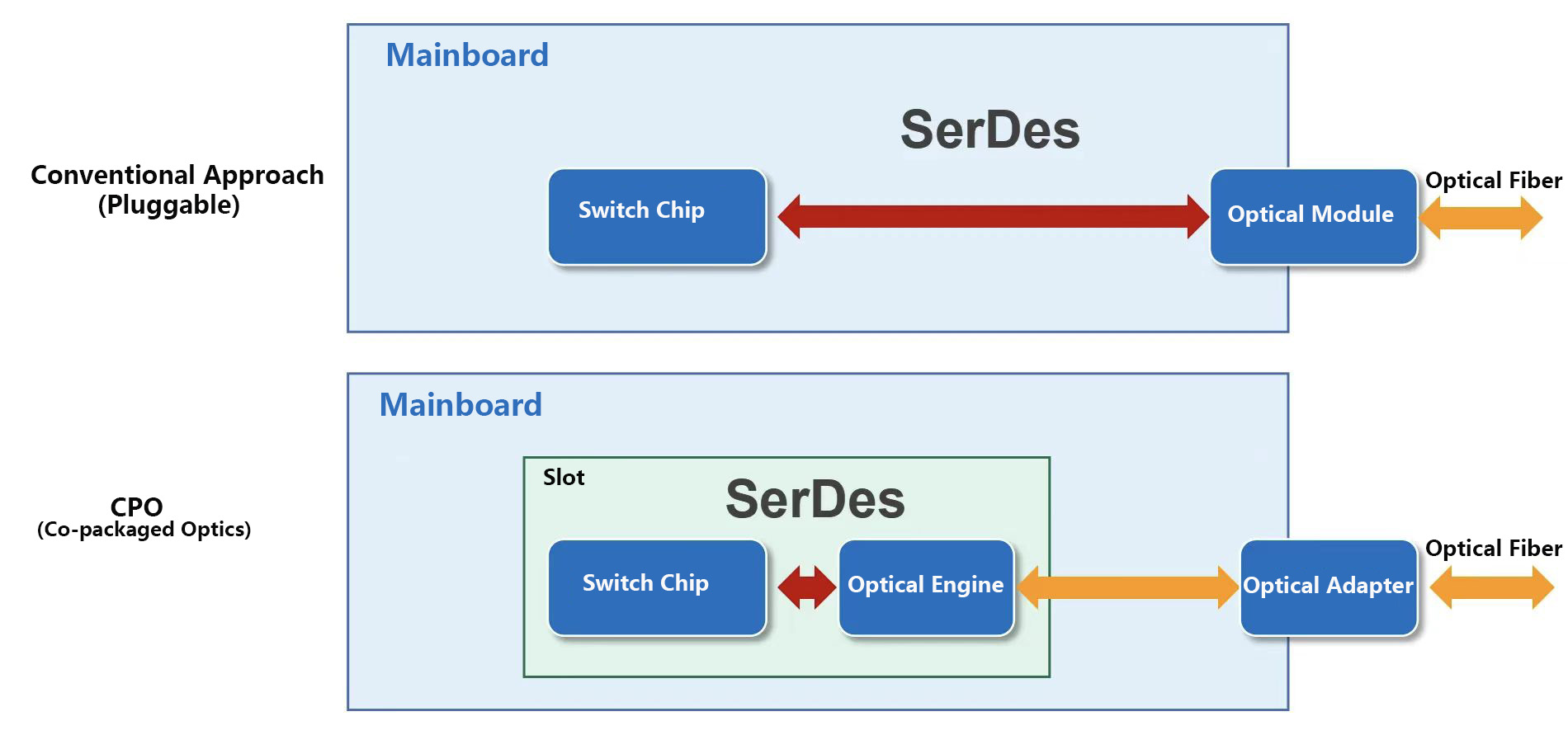
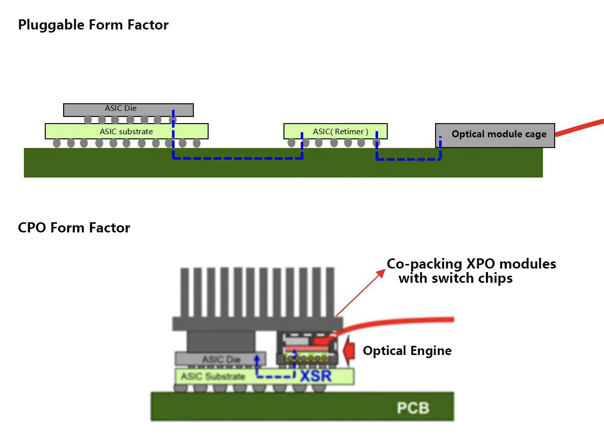
1. Bringing optics closer to the switch ASIC to minimize electrical path losses.
2. Co-packaging optics with switch chips, a approach known as CPO (Co-Packaged Optics).
By leveraging CMOS fabrication techniques, Silicon Photonics enables monolithic integration of optical components like modulators, detectors, and waveguides onto a single silicon chip.
 二、Silicon Photonics Transceivers: Architecture & Advantages
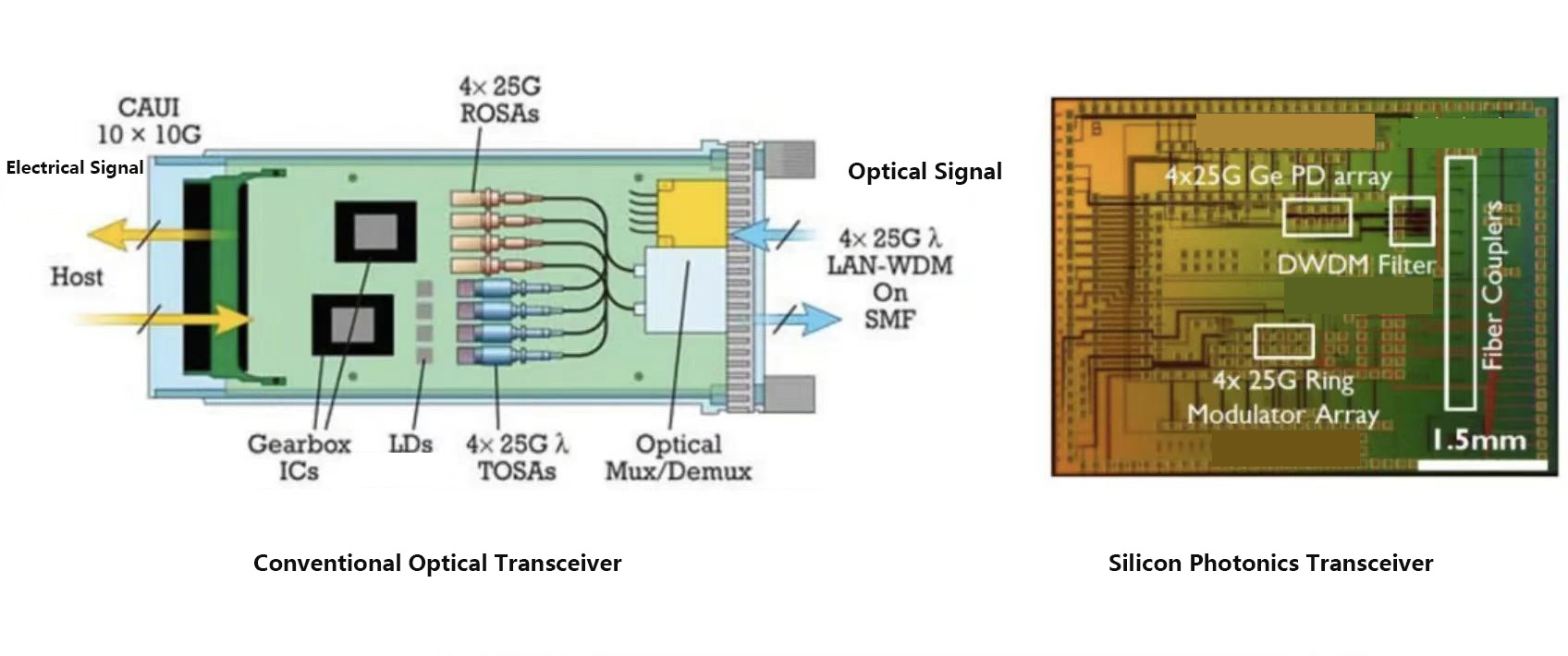
1.Traditional Optical Modules
The primary function of an optical transceiver is to transmit and receive light signals. A traditional optical transceiver houses multiple components, including active devices like the laser (light source), modulator, and detector, as well as passive devices such as lenses, alignment components, and fiber ferrule. During manufacturing, these components are first produced individually and then assembled into a complete module—a process known as "Discrete Device Packaging."
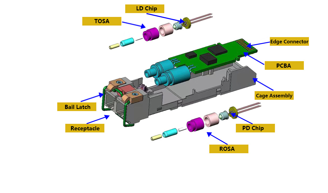
The module contains both electrical and optical chips. Key electrical chips include the Laser Driver (LD), Trans-Impedance Amplifier (TIA), Clock and Data Recovery (CDR) circuit, Main Amplifier (MA), and a sophisticated Digital Signal Processing (DSP) chip. The optical chips are primarily responsible for photoelectric conversion, such as the laser diode chip and detector chip.
2. Silicon Photonics Transceivers
The Silicon Photonics (SiPh) Optical Transceiver is fabricated using standard CMOS manufacturing processes—such as photolithography, etching, and deposition—to build modulators, detectors, and passive optical components directly onto a silicon (Si) substrate. This approach enables a significantly higher level of integration compared to traditional transceivers.
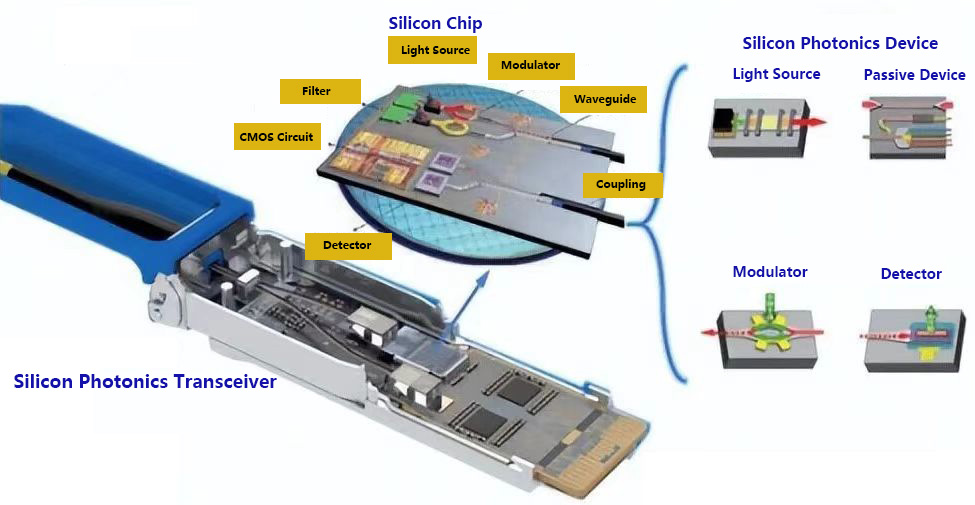
An enlarged view looks like this:
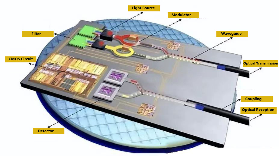
While functionally equivalent to its traditional counterparts in performing electro-optical conversion, the key advantage of the SiPh transceiver lies in its monolithic integration of all components, resulting in a far more compact and efficient design.
400G Silicon Photonics Transceiver Structure(from intel):
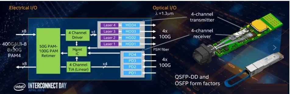
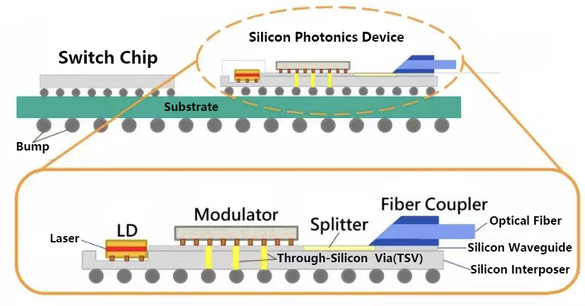
The following illustration depicts the packaged structure of a silicon photonics transceiver:
 三、Key Benefits of Silicon Photonics Transceivers
(1) Higher Integration: Monolithic integration reduces component count and size by ~30%, enabling higher port density for AI clusters and large-scale data centers.
(2)Cost Efficiency: Silicon substrates are significantly cheaper than III-V materials (e.g., InP costs ~20x more).
(3)Lower Power Consumption: Eliminating TEC (Thermoelectric Cooler) and reducing insertion loss cut power usage by ~40% (e.g., 800G transceivers consume ~14W vs. 18W for traditional modules).
(4) Leveraged CMOS Ecosystem: Reusing semiconductor manufacturing processes accelerates scalability and innovation.
四、Challenges in Silicon Photonics Despite its promise, Silicon Photonics faces hurdles:
· Light Source Integration: Silicon’s indirect bandgap requires external lasers, complicating efficient coupling.
· Performance Trade-offs: Silicon modulators may lag behind InP or lithium niobate in bandwidth and drive voltage.
· Process Yield & Reliability: Temperature/humidity fluctuations in data centers demand robust designs, while diverse technical approaches (e.g., waveguide types, fiber arrays) hinder standardization.
· Immature Ecosystem: Limited industry standards and customization needs slow mass adoption.
五、Applications of Silicon Photonics(1)Optical Communications: Dominating AI-driven 800G/1.6T transceivers, with estimates suggesting 35–40% market share in 800G and 80% in 1.6T deployments.
(2) LiDAR: Enables compact, solid-state LiDAR for autonomous vehicles and industrial automation.
(3)Optical Computing: Silicon photonic chips accelerate matrix operations in AI workloads with unparalleled energy efficiency.
(4)Bio-sensing: High-sensitivity, portable sensors for medical diagnostics and environmental monitoring.
六、Conclusion Silicon Photonics fiber optical transceivers are pivotal for next-generation data centers, offering unmatched scalability, power efficiency, and cost savings. As the industry races toward 3.2T and CPO solutions, Silicon Photonics will play a critical role in shaping the future of high-speed connectivity. As a manufacturer with many years of experience in the optical communication industry, HYTOPTODEVICE hope to work with you to drive industry development and progress together in the interconnected world!


