
Modern AI training widely employs hybrid strategies of data parallelism and model parallelism:
Data Parallelism: Batch data is split across multiple GPUs, requiring frequent All-Reduce operations for gradient synchronization.
Model Parallelism: The model itself is partitioned across GPUs, creating forward/backward propagation pipelines.
Both modes generate intensive point-to-point communication patterns. Each iteration is like a precise relay race where any delay in a single leg slows down the entire team.
According to Amdahl's Law, system speedup is limited by its serial portion. In AI training, communication is that unavoidable "serial portion." While GPU computing power grows exponentially yearly (from A100 to H100 to B200), improvements in network latency progress relatively slowly, making communication bottlenecks increasingly prominent.
Training a GPT-4-level model: Requires approximately 25,000 GPUs running for 90–100 days.
A 10% optimization in communication latency: Could save about 10 days of training time.
Cost savings: Millions of dollars in electricity alone, not to mention the competitive advantage of earlier market entry.
Higher speeds naturally reduce per-bit transmission time:
100G optical module: 10 ps per bit.
800G optical module: 1.25 ps per bit.
However, speed upgrades alone cannot solve all latency issues. Optimizing response time is equally critical.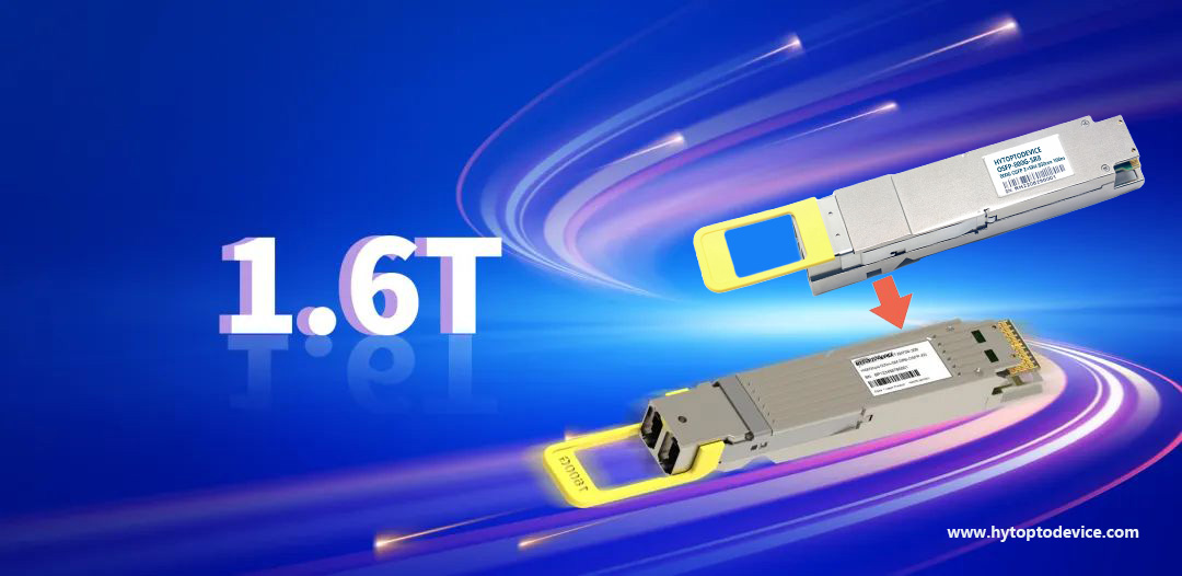
As a professional optical module manufacturer, HYTOPTODEVICE achieves low latency through the following technological innovations:
Material-Level Optimization
Self-developed laser chips: Using Directly Modulated Lasers (DML) instead of external modulation schemes to reduce modulation steps.
Custom driver chips: Optimizing driver circuit response times to minimize signal shaping delays.
Advanced packaging processes: Shortening inter-chip interconnect distances to reduce parasitic effects.
Design-Level Innovations
Simplified DSP workflows: Optimizing Forward Error Correction (FEC) schemes for short-distance AI training scenarios (<100 meters), reducing processing latency while ensuring bit error rates.
Predictive activation technology: Anticipating data flow arrival times to prepare laser states in advance.
Pass-through architecture: Minimizing internal buffering for near-line-rate forwarding.
Manufacturing-Level Control
Full vertical integration: End-to-end control from chips and components to modules, ensuring process consistency.
100% factory latency testing: Each optical module undergoes precise response time measurement.
Batch stability assurance: Self-sufficient material supply chain with performance fluctuations controlled within ±5%.
Co-Packaged Optics (CPO) integrates optical engines and switch ASICs within the same package, reducing electrical interconnect distances by up to 90%. This is expected to bring latency down to below 10 ns. However, CPO faces challenges in maintainability, thermal management, and standardization, and is expected to coexist with pluggable solutions for the next 3–5 years.
Linear-Drive Pluggable Optics, as an intermediate approach, removes DSP chips and shifts analog signal processing functions to the switch side. This can reduce DSP processing latency by approximately 20 ns while retaining the advantages of pluggability.
CPO Form Factor Transceiver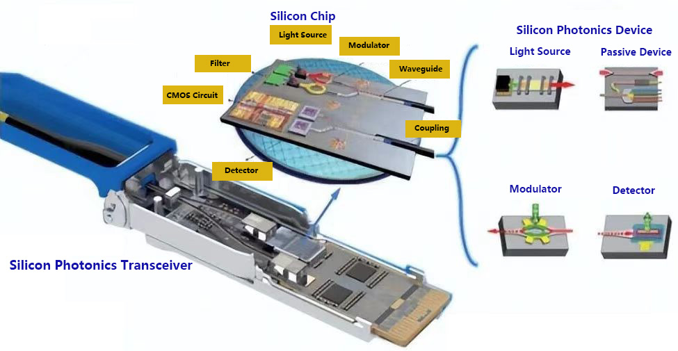
Specifically optimized for AI/ML scenarios, our low-latency optical modules include:
800G SR8 : For intra-rack data center interconnects, latency <100 ns.
800G DR8 : For intra-building data center interconnects, latency <120 ns.
400G FR4 : For cost-performance priority scenarios, latency <80 ns.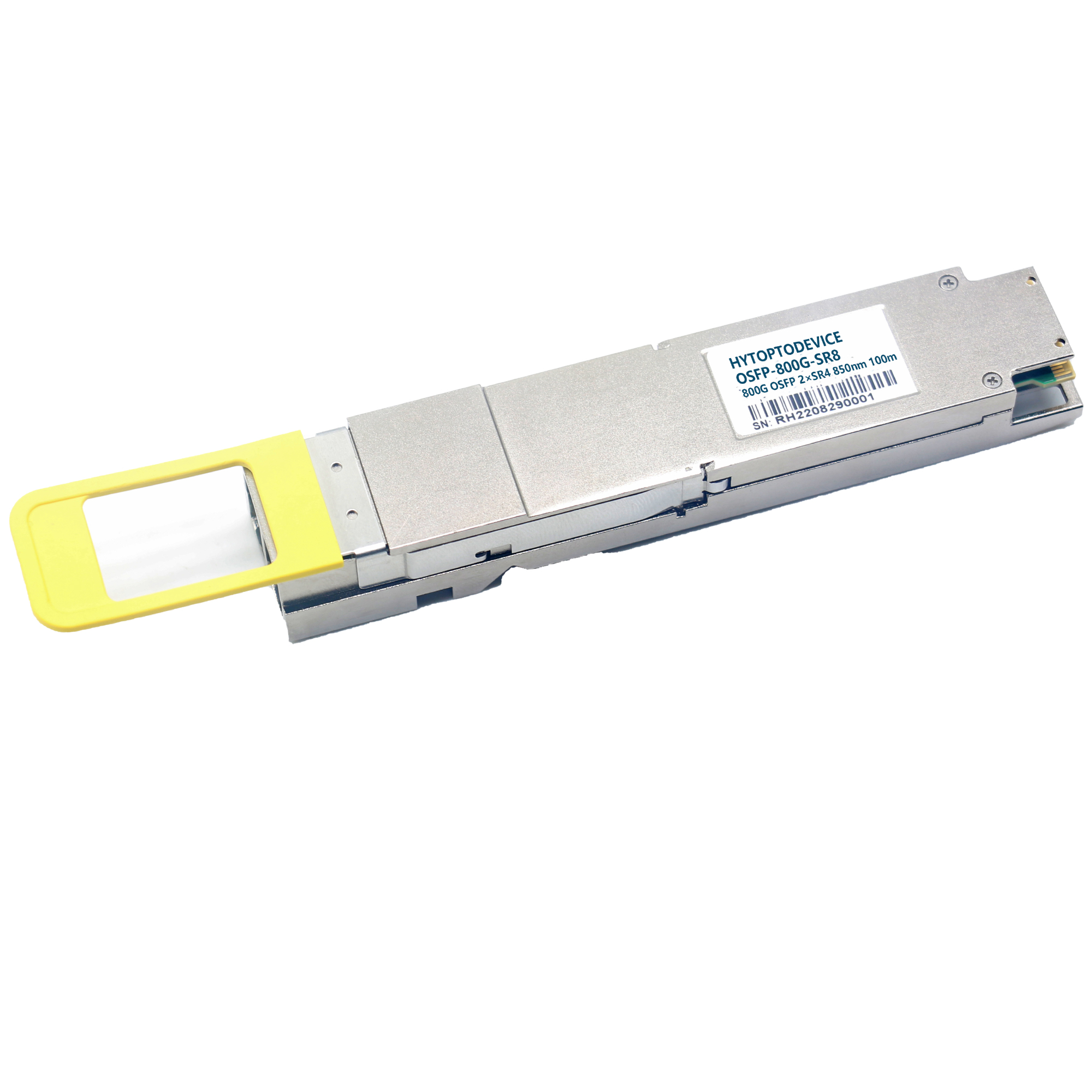
For ultra-short-distance (<5 meters) GPU cluster interconnects, our high-speed cables provide near-zero latency solutions:
800G DAC: Passive copper cables with negligible latency (<1 ns).
800G AOC: Active Optical Cables with latency <50 ns, offering both distance and flexibility.
We maintain deep partnerships with leading AI accelerator manufacturers, providing:
Optical modules optimized for NVIDIA Quantum-2 InfiniBand.
Compatibility testing for RoCE v2 and GPUDirect RDMA.
Custom latency profiles tailored to specific cluster topologies.
Latency budget allocation: Define end-to-end latency targets for the cluster and derive optical module requirements accordingly.
Transmission distance needs: Intra-rack, intra-building, or campus-wide? Distance determines technology selection.
Topology adaptation: Fat-Tree, Dragonfly+, or Hypercube? Different topologies have varying sensitivities to link latency.
Future scalability: Plan for seamless evolution to 1.6T and beyond.
Before deployment, we recommend:
End-to-end latency testing: Measure actual latency using precision instruments.
Traffic pattern simulation: Simulate typical AI training traffic patterns like All-Reduce and All-to-All.
Long-term stability testing: Verify latency stability under high temperatures and heavy loads.
As AI training enters the era of "10,000-card clusters," communication efficiency has become a critical determinant of training cost and speed. Though small, low-latency optical modules are the "super synapses" connecting these vast computing clusters, directly determining whether trillion-parameter models can "think" efficiently and collaboratively.
As an optical module manufacturer with full vertical integration capabilities, HYTOPTO DEVICE provides stable, high-performance, and rapidly deliverable communication solutions for AI infrastructure—from 1G to 800G, from pluggable modules to high-speed cables. Our self-sufficient material supply chain and end-to-end controlled production processes ensure every optical module delivers exceptional latency characteristics and reliability.
In the "race against time" of AI competition, every nanosecond is worth fighting for. Choosing the right optical module is purchasing the most critical "time insurance" for your valuable computing resources.


